

 Product
 Brand
Brand Articles
 Tools
Tools
MCU Crystal Selection & Startup Verification: Load Capacitance, ESR, and Oscillation Margin Guide
When a microcontroller (MCU) fails to boot in an environmental test chamber, drops clock synchronization across specific manufacturing batches, or refuses to run after a bill-of-materials (BOM) component substitution, the root cause is rarely a defective silicon chip. In the overwhelming majority of cases, the failure stems from a mismatched Pierce crystal oscillator circuit.
A quartz crystal resonator is not a digital plug-and-play component. It is an electro-mechanical transducer embedded in an analog amplifier loop. Sizing and validating this circuit requires balancing load capacitance (), Equivalent Series Resistance (ESR), active transconductance (), and drive level power dissipation ($DL$).
In a standard Pierce oscillator circuit, the microcontroller silicon boundary houses the active inverting amplifier alongside an internal feedback bias resistor () connected across the OSC_IN and OSC_OUT pins. Externally, the circuit is completed by the quartz crystal resonator, an optional series damping resistor () located at OSC_OUT, two discrete load capacitors (and) referenced to ground, and the inevitable PCB and package stray capacitance ().
Executive Summary: The 5-Point Crystal Selection Protocol
Before freezing an MCU schematic or approving an alternate crystal part number for production, hardware and component engineers must verify five electrical boundary conditions:
Target Frequency and Total Tolerance Budget: Ensure the crystal’s total frequency deviation—combining calibration tolerance at, temperature drift across the target operating range (e.g.,or), and multi-year aging—falls within peripheral communication specifications (e.g.,for CAN,for standard USB 2.0 Full Speed, orfor Bluetooth Low Energy).
Load Capacitance Matching (): Calculate external load capacitors () by accounting for multi-layer PCB routing parasitics and MCU pin capacitances (). Never set.
Gain Margin and Oscillation Safety Factor ($SF$): Confirm that the MCU inverter's transconductance () comfortably exceeds the critical transconductance () demanded by the crystal's maximum ESR and shunt capacitance (). Physical benchtop negative resistance testing must demonstrate an Oscillation Safety Factor offor High-Speed External (HSE) clocks andfor Low-Speed External (LSE,) clocks.
Drive Level ($DL$) Dissipation: Verify that the excitation power delivered by the MCU does not exceed the maximum physical rating of the quartz blank (), adding an external series damping resistor () on the inverter output pin when required.
Dielectric Integrity: Mandate Class 1 C0G (NP0) ceramic capacitors for the external tuning tank. Never permit Class 2 dielectrics (X7R, X5R) in crystal circuits.
1. The Pierce Oscillator Architecture: Inverter, Resonator, and Barkhausen Loop Gain
The dominant oscillator topology implemented inside modern microcontrollers is the Pierce oscillator. It consists of an internal unbuffered CMOS inverter, an internal or external high-value feedback bias resistor (), and an external-network formed by the quartz crystal and two discrete load capacitors.
The quartz resonator can be electrically modeled as two parallel paths: a motional arm containing the series motional inductance (), motional capacitance (), and motional resistance (, representing ESR), placed in parallel with a shunt arm representing the physical electrostatic plate and package capacitance ().
Inverter Self-Biasing and Phase Shift Conditions
For sustained oscillation, Barkhausen's criterion requires a loop gain equal to or greater than unity () and a total closed-loop phase shift of exactly(or) at the operating frequency:
Internal Amplifier Phase Shift (): The MCU's internal CMOS inverter providesof phase inversion between the input (
OSC_IN) and output (OSC_OUT).Linear Operating Region: The feedback resistor(typically) provides DC negative feedback around the inverter, biasing the input and output voltages to approximately half the supply rail (). In this high-gain linear region, microscopic thermal noise is amplified to trigger oscillation.
External-Network Phase Shift (): The quartz resonator behaves as an inductive reactance at its operating point, forming a-network with external capacitorsand. This network contributes the additionalof phase shift, satisfying thepositive feedback condition.
The Butterworth-van Dyke (BVD) Model
A quartz resonator cannot be analyzed purely as a standard filter component. Electrically, it operates according to the Butterworth-van Dyke (BVD) equivalent circuit[7]:
Motional Inductance (): Models the vibrating mechanical mass of the quartz blank (typically Henries to kilo-Henries).
Motional Capacitance (): Models the mechanical elasticity (compliance) of the quartz element (typically femto-Farads).
Motional Resistance (): Represents internal friction and acoustic energy losses in the quartz material and its physical mounting structure.
Shunt Capacitance (): The purely electrostatic capacitance formed between the metal electrode platings on opposite faces of the blank, plus the parasitic capacitance of the crystal package leads/holder (typically).
Series () vs. Parallel Load () Resonance
A crystal resonator has two zero-phase resonant frequencies:
Series Resonant Frequency (): Occurs where the reactive impedances ofandcancel out:At this point, the crystal's electrical impedance is purely resistive and minimal ().
Anti-Resonant Frequency (): Occurs where the inductive motional arm resonates in parallel with the shunt capacitance, resulting in an impedance peak.
Microcontroller Pierce oscillators operate in the inductive region bounded betweenand. When placed in series with the external circuit load capacitance (), the crystal resonates at its nominal parallel load resonant frequency ():
Becauseis an explicit function of, any mismatch between the actual circuit capacitance and the crystal's specifieddirectly pulls the operating frequency away from its nominal target.
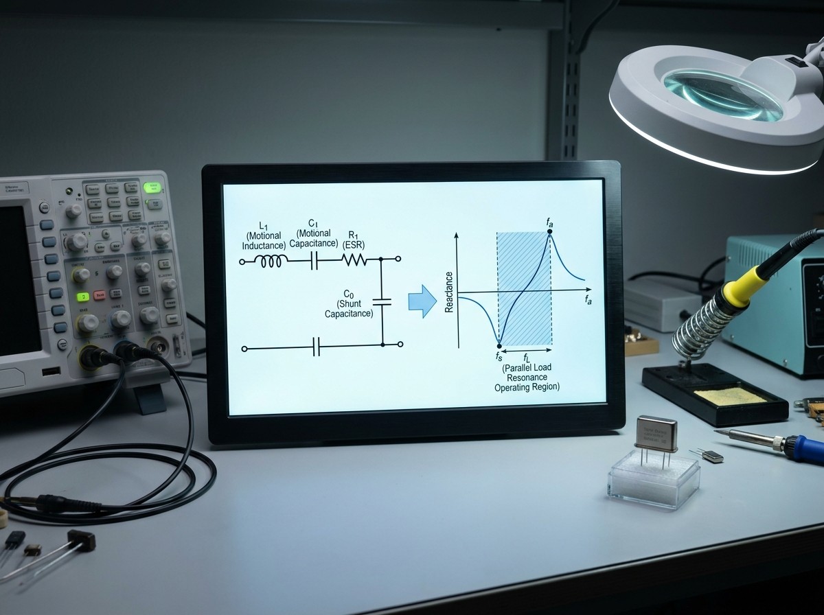
2. Matching Load Capacitance (): Mathematical Derivation and Stray Estimation
The specified load capacitance () in a crystal's datasheet is not the value of the capacitors soldered onto the board. It is the net equivalent capacitance that the quartz crystal must "see" looking outwards across its two terminals.
Mathematical Derivation of External Capacitors
In the Pierce topology, external capacitorsandappear in series with respect to the crystal's terminals, in parallel with all board and package stray capacitances ():
In standard symmetrical implementations where, the series combination reduces to:
Solving directly for the required external capacitor value:
A pervasive mistake made by junior hardware engineers is assuming. As documented in load capacitance analyses[8], if ancrystal is paired withexternal capacitors on a board with, the effective load seen by the crystal is only. This under-loading error shifts the parallel resonance frequency upward, pulling the clock high and potentially causing clock-sensitive communications to drop frames.
Deconstructing Stray Capacitance ()
Stray capacitance represents the parasitic capacitive paths from the oscillator traces to local ground planes and power nets:
MCU Pin Capacitance (): Package lead frames, bond wires, and internal ESD protection structures introduce parasitic capacitance to ground, typically ranging fromper pin (refer to the MCU datasheet under "I/O pin characteristics").
PCB Trace Parasitics: Microstrip traces routed over an adjacent internal ground plane contribute approximatelyper inch depending on layer stackup thickness, trace width, and clearance.
Component SMT Land Patterns: Solder pads for SMD crystals and ceramic capacitors add roughlyeach.
On a compact, well-routed multi-layer FR4 board,typically settles within an empirical baseline of(STMicroelectronics Application Note AN2867[1] designatesas a standard rule-of-thumb baseline for initial calculations). However,is an empirical estimate, not a universal constant. Dense designs with bottom-side routing, long escape traces, or adjacent copper pours may measure upwards of.
Symmetrical Sizing Calculation Examples
| Design Parameter / Step | HSE Example 1 (Standard 16 MHz) | HSE Example 2 (Low-Cap 24 MHz) | LSE Example (32.768 kHz RTC) |
|---|---|---|---|
| Resonator Target Frequency | |||
| Specified Crystal | |||
| Estimated Layout | (4-layer standard layout) | (Tight, optimized routing) | (Direct adjacent placement) |
| Net Series Capacitance Required | |||
| Ideal Symmetrical Value () | |||
| Selected Standard E24/E96 Value | (actual:) | (actual:) | (actual:) |
Dielectric Selection: Why C0G/NP0 Is Mandatory
The choice of dielectric material forandis critical:
Class 1 (C0G/NP0): C0G (also designated NP0) ceramics utilize non-ferroelectric formulations. They exhibit a flat temperature coefficient offrom, negligible aging, and zero capacitance change across DC bias voltage. They are mandatory for crystal circuits.
Class 2 (X7R, X5R, Y5V): Ferroelectric formulations suffer massive capacitance degradation under DC bias (often losingof rated capacitance at working voltages) and fluctuate wildly across temperature (or worse). Using an X7R capacitor forcauses the oscillator to drift off-frequency when warm and can drop total tank capacitance so low at cold temperatures that the oscillator drops out of regulation.
3. Equivalent Series Resistance (ESR), Transconductance (), and Startup Dynamics
Oscillator startup is fundamentally a transient, small-signal process. At power-on, thermal noise within the quartz resonator generates minute currents that the MCU's internal amplifier must amplify. If the losses inside the circuit exceed the amplifier's gain, the oscillation decays to zero.
Crystal vs Oscillator: Load Capacitance, Accuracy, and Common Design Mistakes | 10 Key Differences
The Physics of Equivalent Series Resistance (ESR)
The motional resistance () represents internal losses at series resonance. However, because the crystal operates with external capacitive loading at parallel resonance (), the effective series resistance that the MCU amplifier must overcome is higher than. This is the Equivalent Series Resistance (ESR):
As quartz packages shrink physically (e.g., transitioning from legacy 5032 or 3225 footprints down to 2016 or 1612 sizes), their ESR rises dramatically. Acrystal in a 3225 package typically exhibits an ESR around. The exact same frequency in a 1612 package often exhibits an ESR of. Smaller quartz blanks possess less vibrating mass and encounter higher boundary damping, forcing the active silicon to work harder to maintain oscillation.
Critical Transconductance ()
The transconductance () of the MCU inverter represents its ability to convert an input voltage swing into output drive current. As documented in NXP AN14518[2], Barkhausen's gain criterion establishes that sustained oscillation requires the active transconductance to exceed a critical transconductance threshold ():
Where:
is the nominal oscillator operating frequency in Hertz.
is the crystal's maximum equivalent series resistance in Ohms.
is the crystal shunt capacitance in Farads.
is the nominal specified load capacitance in Farads.
From this relationship, the power-law dependencies become clear:scales directly with ESR, with the square of operating frequency (), and with the square of the total capacitance term. Selecting a crystal with an unnecessarily high load capacitance (such as choosinginstead of) exponentially inflates the transconductance required from the MCU.
Gain Margin Requirements
To guarantee immediate, reliable startup across silicon processing corners (fast/slow wafers), power rail sags, and environmental extremes, the MCU's transconductance () must provide substantial headroom over:
High-Speed External (HSE, MHz-range): Industry standards mandate. If, the design risks intermittent startup lockup, long boot delays, or failure at low temperatures.
Low-Speed External (LSE, 32.768 kHz RTC): Because real-time clock oscillators are engineered for ultra-low power consumption (often consuming under), their transconductance is restricted to small bias currents (). Consequently, as highlighted for wireless MCUs[5], low-speed oscillators operate under a reduced gain margin baseline of.
Thermal Compounding: The CMOS transconductancedegrades as ambient temperature rises due to reduced silicon carrier mobility. Conversely, crystal ESR increases at low temperatures. A marginal design that exhibits a calculated gain margin of 2.0 atwill frequently fail to start at cold-boot () or fail during hot-soak ().
4. Drive Level ($DL$) Verification and Series Damping Resistor () Sizing
While insufficient drive results in startup failure, excessive drive destroys the quartz resonator. The Drive Level ($DL$) is the measure of active power dissipated inside the crystal blank, expressed in microwatts ().
Consequences of Overdriving Quartz
Quartz is a piezoelectric crystal subject to mechanical shear stress. Exceeding its rated maximum drive level causes:
Mechanical Stress & Micro-Fracturing: The physical amplitude of the internal acoustic wave exceeds the elastic limits of the quartz crystal lattice, causing micro-cracks at the electrode bonding points or catastrophic mechanical blank fracturing.
Frequency Pulling & Non-Linearities: High drive levels cause thermal expansion of the quartz element, inducing dynamic frequency shifts away from nominal resonance.
Accelerated Aging: Long-term frequency drift over years of operation scales directly with sustained drive level stress.
Modern miniature SMD crystals (e.g., 2016 and 1612 packages) have tiny mechanical volumes, restricting their maximum permissible drive level to(compared tofor legacy 5032 packages). Ultra-low-powertuning-fork crystals are even more delicate, typically specified for maximum drive levels of.
Calculating and Measuring Drive Level
Drive level is governed by the classic power dissipation equation across the crystal's equivalent resistance:
Whereis the root-mean-square alternating current flowing through the quartz resonator.
Direct measurement requires assessing current flow through the resonator. In laboratory environments, an RF current probe clamped over a small wire loop soldered in series with the crystal between OSC_OUT (downstream of any damping resistor) and the crystal blank allows non-intrusive current acquisition.
Direct Bench Measurement (RF Current Probe): As outlined in drive level measurement guides[4], the most accurate verification technique involves lifting a crystal pin, inserting a small wire loop, and measuringdirectly using a high-frequency current probe connected to an oscilloscope or RF spectrum analyzer.
Indirect Mathematical Approximation (Voltage Swing Method): If an RF current probe is unavailable,can be estimated by measuring the peak-to-peak voltage () at the crystal's input terminal (node) using an ultra-low-capacitance active FET probe:Substituting back into the drive level formula:
Sizing the External Series Damping Resistor ()
If the calculated or measured drive level exceeds the crystal’s rated limit (), a discrete series damping resistor () must be inserted into the circuit.
Placement Rules: The damping resistormust always be placed on the inverter output side (
OSC_OUT), between the MCU pin and capacitor. It must never be placed on theOSC_INside. Placing it atOSC_OUTisolates the inverter's low output impedance from the capacitive tank and attenuates drive current, whereas placing it onOSC_INadds noise and degrades phase shift into the amplifier input.First-Order Sizing Rule: The impedance ofshould approximate the capacitive reactance ofat resonance:Typical empirical values range fromfor high-speed MHz oscillators.
The Engineering Compromise: Sizingis a balance between reliability and startup margin. Inserting an oversizeddrops crystal dissipation safely below, but it simultaneously increases total loop series resistance, degrading the circuit's negative resistance and starving startup margin.
5. Physical Bench Verification: The Negative Resistance ($-R$) Test Protocol
Theoretical calculations and SPICE simulations are essential starting points, but they cannot account for silicon lot transconductance spread, board-level trace coupling, and temperature-induced impedance shifts. Every embedded design must undergo physical hardware verification using the Series Substitution Method to establish its real-world Oscillation Safety Factor.
In this verification setup, a variable or selectable discrete non-inductive resistoris placed in series between the quartz crystal resonator and the microcontroller's OSC_IN pin, with load capacitorremaining connected at the inverter input node.
Laboratory Standard Operating Procedure (SOP)
The negative resistance ($-R$) measurement[6] of an active oscillator circuit represents the net dynamic negative impedance supplied by the MCU amplifier to cancel the positive loss resistance (ESR) of the resonator.
Board Preparation: On a functional prototype PCBA, cut the trace leading from the crystal terminal to the MCU's
OSC_INpin. Solder a two-terminal surface-mount pad or micro-trimmer placeholder in series with the trace.Baseline Confirmation: Place a zero-ohm link (). Power on the board and confirm steady-state oscillation.
Iterative Resistance Stepping: Replacewith non-inductive SMD resistors of progressively increasing values (e.g.,). Avoid wire-wound or axial leaded resistors, as their parasitic inductance alters the resonant loop.
Hard Power-Cycle Verification: At every resistance step, perform a minimum of 10 to 20 hard power cycles (switchingcleanly fromto nominal). Do not evaluate margin by observing an already-running oscillator; the circuit must demonstrate the ability to self-start from a cold stop.
Identifying: The value ofwhere the oscillator either fails to start within the specified boot delay or fails to start entirely across the test cycles designates the operational cutoff. The last verified reliable value is defined as.
Calculating Total Negative Resistance ($|-R|$):
Determining the Oscillation Safety Factor ($SF$): Compare the circuit's total negative resistance against the crystal's worst-case maximum ESR specified across temperature:
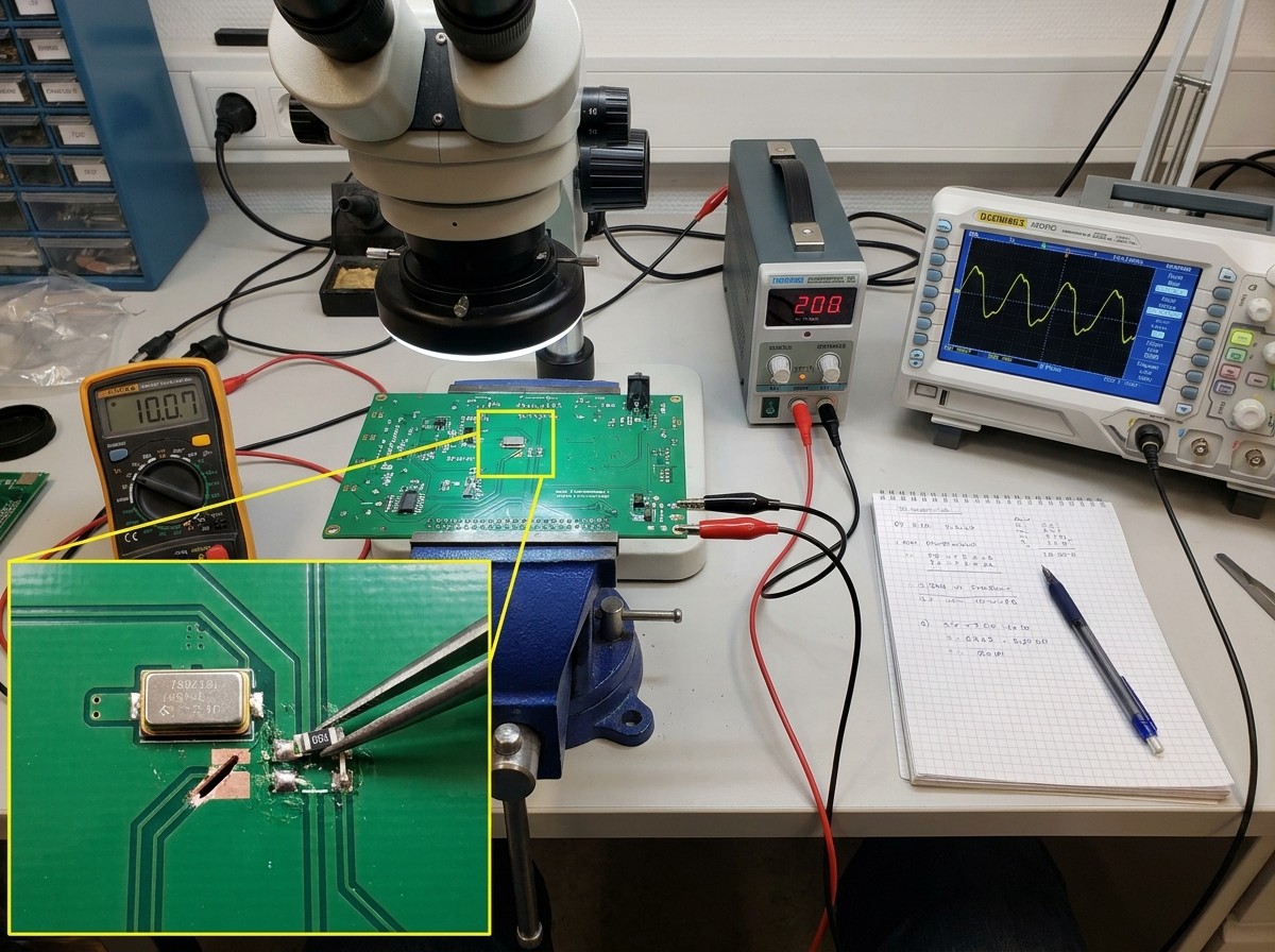
Pass/Fail Decision Matrix
According to oscillation margin standards[3], measured safety factors dictate field viability:
| Safety Factor ($SF$) | Operational Status | Production Risk Level | Mandatory Engineering Action |
|---|---|---|---|
| Fail | Critical: Extremely high risk of random field boot failures, assembly line yield dropouts, and cold-boot locks. | Do not release to production. Redesign circuit immediately: decrease external, select a crystal with lower ESR, adjust MCU firmware drive settings to higher transconductance, or shorten PCB traces. | |
| Marginal / Conditional Pass | Medium: Unacceptable for high-speed MHz clocks. Tolerable only for ultra-low-powerRTC oscillators in benign indoor operating environments. | For HSE circuits: Re-spin or adjust matching components. For LSE circuits: Perform extended temperature sweeps () to guarantee zero dropouts. | |
| Standard Pass | Low: Proven robust design for commercial, industrial, and consumer IoT hardware. | Production-ready. Qualify alternate crystal sources using identical negative resistance bench validation. | |
| High-Reliability Pass | Negligible: Meets the stringent demands of automotive (AEC-Q100/Q200), medical life-support, and aerospace hardware. | Sign off on production BOM. Demonstrates complete immunity to voltage sags, temperature limits, and multi-year aging. |
6. The "Identical Package & Frequency" Sourcing Fallacy
A frequent failure mode in high-volume electronics manufacturing occurs when procurement or component engineers cross-reference crystals based purely on center frequency (e.g.,) and package footprint (e.g., 3225 4-pad SMD). Treating quartz resonators as commodities leads directly to factory line stops.
Dissecting Two "Equivalent" 16 MHz 3225 Crystals
| Specification Parameter | Original Component (Part A) | Second-Source Candidate (Part B) | Circuit Impact of Direct Substitution |
|---|---|---|---|
| Nominal Frequency | Center frequency matches perfectly. | ||
| Footprint / Dimensions | (SMD 3225) | (SMD 3225) | Land pattern is pin-compatible. |
| Specified Load Capacitance () | Frequency Detuning: The existing circuit'sload capacitors leave Part B drastically under-loaded. Part B oscillates far above nominal frequency, causing UART bit timing errors and RF packet corruption. | ||
| Max ESR () | Loop Gain Collapse: Asurge in ESR drivesabove the MCU inverter's capacity. Oscillation Safety Factor plummets fromto, causing intermittent startup failure at cold boot. | ||
| Max Drive Level () | Overdrive Burnout: Part A's circuit suppliesof drive power. Part B is rated formaximum, leading to internal lattice stress, accelerated aging, and physical micro-fractures. | ||
| Shunt Capacitance () | Further escalates the critical transconductance requirement (). |
Component Engineer's Cross-Reference Checklist
Before approving any alternate or second-source crystal part number on an active BOM, verify the following:
[ ] Load Capacitance Alignment: Does the replacement match the originalwithin? If not, are the engineering teams prepared to change thecapacitor values on the SMT feeder line?
[ ] Maximum ESR Parity: Is the replacement part’s maximum ESR equal to or lower than the original specification across the entire operating temperature range? ().
[ ] Maximum Drive Level Ceiling: Does the replacement's ratedsafely exceed the measured drive power delivered by the circuit?
[ ] Physical Shunt Capacitance (): Islow enough to preserve required transconductance margins?
[ ] Laboratory Re-Verification: Has the proposed substitute undergone physical negative resistance bench testing (verification) on at least three target PCBAs?
7. Environmental Sweeps, Voltage Sag, and Production Validation Checklist
An oscillator operating reliably on a heated lab bench atcan fail in the field when powered by a dying battery at sub-zero temperatures. High-reliability mass production requires validating the oscillator circuit against environmental and electrical extremes.
The Physics of Temperature Extremes
High-Temperature Roll-off (): Inside the MCU silicon, rising temperatures degrade carrier mobility in the inverter's MOSFET channels. This causes the amplifier's transconductance () to roll off by, eroding startup gain margin.
Low-Temperature ESR Elevation (): The internal acoustic losses in quartz mountings rise at sub-zero temperatures, elevating ESR. Fortuning-fork crystals, parabolic temperature coefficients () produce significant negative frequency pull at.
The 4-Stage Production Qualification Matrix
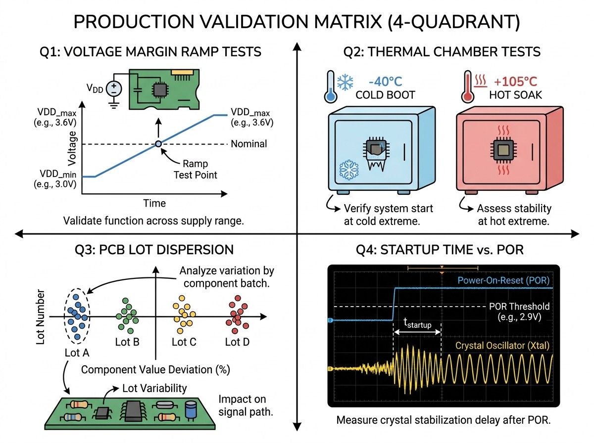
A rigorous manufacturing qualification flow passes sequentially through four test vectors: Stage 1 evaluates supply rail voltage margins and slow ramp times; Stage 2 subjects hardware to cold-boot and hot-soak thermal chamber profiles; Stage 3 inspects component lot and layout dispersion across multiple SMT batches; and Stage 4 characterizes startup delays against internal Power-On-Reset timeouts.
Supply Rail Margin Sweep:
Test oscillator startup at nominal voltage (), absolute minimum operational rail (, typically $10\%$ below nominal), and maximum rail ().
Evaluate slow supply rise times (). When power rails rise slowly, an internal inverter can get trapped in its linear self-biased state, burning quiescent current without generating sufficient noise energy to initiate oscillation.
Thermal Chamber Extremes Soak:
Cold-Boot Cycling: Soak unpowered boards atfor a minimum of 60 minutes. Apply a hardstep and confirm reliable oscillation startup across 50 consecutive cycles.
Hot-Soak Run: Soak boards atorfor 60 minutes. Verify frequency stability and confirm that the MCU inverter's reducedmaintains stable feedback.
Component Lot Dispersion Sweep:
Build and bench-test 5 to 10 prototype units populated from distinct component manufacturing lots (varying MCU silicon wafer fabrication lots, different capacitor manufacturing batches, and separate crystal date codes).
Verify that layout stray capacitance remains uniform across PCBA fabricators.
Oscillation Startup Time Characterization:
Measure the startup duration ()—defined as the time from the application ofreaching $90\%$ of nominal until the clock waveform reaches stable, full-amplitude oscillation.
Cross-referenceagainst the MCU's internal Power-On-Reset (POR) or external hardware reset supervisor timeout. Ensure that hardware reset release delays exceed worst-case crystal startup time by a safety margin of at least.
8. Common Engineering Mistakes and Debugging Traps
The "PCB Astrology" Trap
Arbitrarily placingceramic capacitors on every crystal circuit regardless of frequency or crystal specifications is one of the most common design traps in embedded hardware. For modern low-power microcontrollers and low-crystals, standardcapacitors heavily overload the loop, pulling frequencies off-target and starving startup loop gain. Every design must be calculated based on its specific parameters.
The "3 pF Constant" Fallacy
Blindly assuming that PCB stray capacitance is alwayswithout examining the design's physical implementation invites trouble. A 2-layer FR4 board with wide, unshielded traces running over a distant ground plane may exhibitof stray capacitance. Conversely, a high-density 6-layer HDI layout with narrow microstrip traces running directly over a ground reference layer separated by a thindielectric can easily develop.
The Oscilloscope Probe Loading Trap
Attempting to verify crystal startup by touching a standardpassive oscilloscope probe directly to OSC_IN or OSC_OUT introduces two measurement artifacts:
A standardpassive probe introducesof shunt capacitance and aload to ground.
The False Negative: Touching the probe to a marginal oscillator adds massive capacitive loading, killing the loop gain and causing an otherwise functional oscillator to stall.
The False Positive: On an unstable circuit that is stalled due to insufficient load capacitance, the probe's addedcan artificially tune the tank, causing the oscillator to run only while the probe is touching the pin.
How to Measure Correctly:
Use Internal Buffered Outputs: Configure the MCU's firmware to route the internal system clock to an external digital general-purpose I/O pin (e.g., STM32 Master Clock Output / MCO, or MCU CLKOUT). This provides a zero-load window into oscillator performance.
Active FET Probes: If the crystal pins must be inspected directly, use an active FET probe with an input capacitance of less than() and an input resistance of.
Near-Field Sniffer Loop: Hover an insulated magnetic-field near-field loop antenna (connected to a spectrum analyzer or 50-ohm oscilloscope input) a few millimeters above the crystal package. This detects radiated RF resonance without physical electrical contact.
Third-Harmonic Overtone Latch-Up
High-frequency AT-cut crystals are typically cut to operate at their fundamental vibration mode. However, crystals also possess mechanical overtone modes (3rd, 5th, and 7th harmonics). If an MCU features high internal transconductance () extending well into high frequencies, combined with poorly chosen external load capacitors that lower fundamental impedance, the oscillator circuit can jump mode and start up at its 3rd overtone (e.g., acrystal oscillating at). Sizing an external damping resistoror slightly increasingacts as a low-pass filter, suppressing high-frequency loop gain and ensuring fundamental-mode startup.
Frequently Asked Questions (FAQ)
Why does my oscillator stop running the moment I connect an oscilloscope probe?
Standardpassive oscilloscope probes addof parasitic capacitance and aresistive path to ground. When attached to the high-impedance OSC_IN node, this extra capacitance alters the feedback phase and detunes the-network, while the resistive loading drains energy from the resonant tank. This drops the loop gain below unity, stalling the oscillator. To measure non-intrusively, route the clock out through an internal buffered digital pin (e.g., MCO on STM32) or inspect the pins using an active FET probe withinput capacitance.
Why does my crystal start reliably at room temperature but fail cold boot at -40°C?
At sub-zero temperatures (), the mechanical motional resistance and Equivalent Series Resistance (ESR) of quartz resonators increase due to acoustic loss shifts. If your circuit has an insufficient Oscillation Safety Factor at room temperature (), the elevated cold ESR drives the critical transconductance () above the MCU inverter's transconductance (). The loop gain drops below unity, preventing the oscillator from building amplitude from thermal noise.
Can I intentionally use asymmetrical load capacitors ()?
Yes. While symmetrical loading () is the standard starting baseline, deliberate asymmetry is sometimes used by experienced RF engineers. Setting(on the OSC_OUT inverter driver side) slightly smaller than(on the OSC_IN amplifier input side) increases the feedback voltage swing delivered into the MCU amplifier. This boosts loop gain and reduces power dissipation inside the crystal blank. However, substantial asymmetry increases waveform distortion and harmonic generation, so it must be bench-validated across voltage and temperature.
Why is the standard RTC crystal frequency always 32.768 kHz?
is an exact mathematical power of two (). By feeding this frequency into a simple 15-stage binary ripple counter (where each stage divides the input frequency by 2), the MCU hardware produces an exacttimebase with minimal silicon logic gates. Tuning-fork crystals cut tocan also be manufactured in miniature sizes while drawing operating currents in the nanoampere range, making them suitable for battery-backed real-time clock (RTC) circuits.
How do I know if my design requires an external series damping resistor ()?
An external series damping resistor () is required when the measured or calculated drive level () exceeds the maximum drive level limit specified in the crystal’s datasheet. This is common when pairing modern, high-transconductance microcontrollers with small-package SMD crystals (such as 2016 or 1612 sizes, which typically have a limit of). If your calculated drive level exceeds this ceiling, place anon the OSC_OUT pin (typically) to attenuate drive current, and verify that the remaining Oscillation Safety Factor still meets or exceeds.
Sources and references used for this guide
Guidelines for oscillator design on STM8AF/AL/S and STM32 MCUs/MPUs (AN2867)
Source type: official company documentation
Used for: Pierce oscillator theory, critical transconductance (gm_crit) formulas, HSE vs. LSE safety factor thresholds (SF >= 5 vs SF >= 3), external capacitance calculations.
Caution: Vendor technical application note. Calculations are optimized for STMicroelectronics oscillator architectures, but physical principles generalize across all Pierce oscillators.Crystal Oscillator Design Guide (AN14518)
Source type: official company documentation
Used for: Negative resistance definitions, drive level equations, oscillator stability analysis, and series resistor tuning procedures.
Caution: Vendor application note. MCU-specific pin capacitance and transconductance parameters must be substituted from the target MCU datasheet.Basic Knowledge of How to Measure the Oscillation Margin
Source type: official company documentation
Used for: Oscillation margin definition, physical laboratory step-by-step SOP for series resistor (Rx) insertion, and pass/fail safety factor criteria.
Caution: Passive component manufacturer reference; focuses on quartz resonator behavior rather than active MCU internal amplifier architecture.Basic Knowledge of How to Measure the Drive Level
Source type: official company documentation
Used for: Drive level physical power dissipation formulas, current probe test setups, and damping resistor sizing.
Caution: Requires precise RF current measurement equipment; indirect voltage swing calculation should be treated as an engineering approximation.Crystal Oscillator and Crystal Selection for the CC13xx, CC26xx, and CC23xx Family of Wireless MCUs (SWRA495)
Source type: official company documentation
Used for: Trade-offs in ultra-low-power wireless microcontrollers, negative resistance safety factors, and load capacitance impacts on battery drain.
Caution: Tailored toward low-power RF microcontrollers operating with sub-milliampere oscillator budgets.AN-802 Crystal-Measuring Oscillator Negative Resistance
Source type: official company documentation
Used for: Physical test bench configuration for measuring negative resistance in embedded microcontroller circuits.
Caution: Requires careful attention to test lead parasitics during discrete component substitution on high-frequency designs.Oscillation Circuit & Examination Method
Source type: official company documentation
Used for: Quartz resonator equivalent electrical parameters (C0, C1, L1, ESR), oscillation loop margin verification, and drive power constraints.
Caution: Focuses on resonator physical properties rather than semiconductor inverter modeling.The Impact of Load Capacitance on Crystal Oscillator Designs
Source type: vendor article
Used for: Practical illustration of how selecting high load capacitance crystals penalizes gain margin in low-power systems.
Caution: Commercial component manufacturer blog; useful for design intuition but should be corroborated by formal semiconductor application notes.
 UTMEL
UTMEL
We are the professional distributor of electronic components, providing a large variety of products to save you a lot of time, effort, and cost with our efficient self-customized service. careful order preparation fast delivery service
 Discovering New and Advanced Methodology for Determining the Dynamic Characterization of Wide Bandgap DevicesSaumitra Jagdale15 March 20242841
For a long era, silicon has stood out as the primary material for fabricating electronic devices due to its affordability, moderate efficiency, and performance capabilities. Despite its widespread use, silicon faces several limitations that render it unsuitable for applications involving high power and elevated temperatures. As technological advancements continue and the industry demands enhanced efficiency from devices, these limitations become increasingly vivid. In the quest for electronic devices that are more potent, efficient, and compact, wide bandgap materials are emerging as a dominant player. Their superiority over silicon in crucial aspects such as efficiency, higher junction temperatures, power density, thinner drift regions, and faster switching speeds positions them as the preferred materials for the future of power electronics.
Read More Applications of FPGAs in Artificial Intelligence: A Comprehensive GuideUTMEL29 August 20255503
This comprehensive guide explores FPGAs as powerful AI accelerators that offer distinct advantages over traditional GPUs and CPUs. FPGAs provide reconfigurable hardware that can be customized for specific AI workloads, delivering superior energy efficiency, ultra-low latency, and deterministic performance—particularly valuable for edge AI applications. While GPUs excel at parallel processing for training, FPGAs shine in inference tasks through their adaptability and power optimization. The document covers practical implementation challenges, including development complexity and resource constraints, while highlighting solutions like High-Level Synthesis tools and vendor-specific AI development suites from Intel and AMD/Xilinx. Real-world applications span telecommunications, healthcare, autonomous vehicles, and financial services, demonstrating FPGAs' versatility in mission-critical systems requiring real-time processing and minimal power consumption.
Read More The 2026 Engineer’s Guide: Choosing the Right MCU for Your Next IoT & New Energy ProjectUTMEL30 April 20261683
A comprehensive comparison of 2026's leading MCUs from ST, NXP, and Microchip across power efficiency, processing performance, connectivity, and ecosystems to help engineers select the optimal chip for next-gen IoT and new energy projects.
Read More AI Server Components: Engineering Next-Gen Data Center Hardware for 100kW RacksUTMEL15 May 2026937
The transition from traditional enterprise IT to AI-driven workloads has rendered legacy data center hardware obsolete, forcing infrastructure planners to re-engineer server components for extreme thermal environments.
Read More The Practical Engineer’s Guide to the NE555N Timer: Pinout, Setup, and TroubleshootingUTMEL29 May 2026712
This comprehensive guide explores the NE555N timer, detailing its 8-pin layout, internal architecture, and key datasheet specifications. It compares the bipolar IC to CMOS variants and details setup configurations for astable, monostable, and bistable modes. Additionally, the guide offers practical troubleshooting advice to prevent common breadboard failures, such as floating reset pins and electrical noise issues.
Read More
Subscribe to Utmel !
![FM31L276-G]() FM31L276-G
FM31L276-GCypress Semiconductor Corp
![MCS3122T-I/ST]() MCS3122T-I/ST
MCS3122T-I/STMicrochip Technology
![SI8230BB-D-IS]() SI8230BB-D-IS
SI8230BB-D-ISSilicon Labs
![HCS365-I/SM]() HCS365-I/SM
HCS365-I/SMMicrochip Technology
![CAP014DG]() CAP014DG
CAP014DGPower Integrations
![FM31278-GTR]() FM31278-GTR
FM31278-GTRCypress Semiconductor Corp
![ACNW3130-000E]() ACNW3130-000E
ACNW3130-000EBroadcom Limited
![ACPL-3130-300E]() ACPL-3130-300E
ACPL-3130-300EBroadcom Limited
![HCS410/P]() HCS410/P
HCS410/PMicrochip Technology
![L9654TR]() L9654TR
L9654TRSTMicroelectronics


